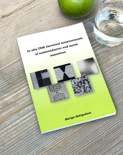
In situ transmission electron microscopy (TEM) is a powerful tool for the field of material science which allows a direct observation of the dynamic response of a material to applied external conditions (electrical bias, heating, reactive environment interaction, etc.) in the real time. In situ TEM experiments provide new knowledge and deep understanding of physic-chemical mechanisms occurring in material at the nanoscale. Unique capabilities of in situ TEM experiments are the result of the recent advancements in the development of TEMs, microelectronics and TEM-holders developed for various external stimulus.
In this thesis we have performed experiments on in situ electrical measurements in order to investigate the behavior of InAs semiconductor nanowires under an influence of applied electric field and study an electromigration phenomenon in thin metallic Au-Pd and Au polycrystalline nanowires in order to produce nanogap electrodes with small nanogap sizes for possible applications in molecular electronics. Also, we have performed in situ heating experiments in TEM to study the behaviour of polycrystalline thin bismuth films with low thermal conductivity under in situ heating and electron-beam bombardment. Also, we have developed a clean room fabrication technique, called back side lithography technique. This technique allows to obtain smooth and uniform electron viewing transparent windows with a thickness of several nanometers at certain locations of a thick SiN membrane which is usually used in MEMS-based chips for in situ TEM experiments.
